Semiconductor cleanroom design has become one of the most critical aspects of modern technology. From smartphones and 5G towers to electric vehicles and satellites, semiconductor chips are at the heart of every innovation. Producing these chips requires ultra-controlled environments where even a single dust particle can destroy a wafer.
In this guide, we’ll cover everything you need to know about semiconductor cleanrooms – from design principles and construction steps to maintenance practices and turnkey solutions that help semiconductor fabs meet global standards.
📑 Table of Contents
- Introduction to Semiconductor Cleanrooms
- Why Semiconductor Cleanroom Design Matters
- ISO Standards for Semiconductor Cleanrooms
- Key Elements of Cleanroom Design
- Cleanroom Construction: Step-by-Step Process
- Modular vs Conventional Cleanrooms in Semiconductors
- Turnkey Semiconductor Cleanroom Solutions
- Cleanroom Maintenance & Validation
- Common Challenges in Semiconductor Cleanrooms
- FAQs on Semiconductor Cleanrooms
- Conclusion
1. Introduction to Semiconductor Cleanrooms
A semiconductor cleanroom is a specialized facility where temperature, humidity, and particulate levels are tightly controlled to ensure defect-free chip manufacturing. These environments are designed according to ISO 14644 standards that classify cleanrooms based on the number of particles per cubic meter of air.
-
ISO Class 1: The cleanest environment, allowing no more than 10 particles per cubic meter.
-
ISO Class 5: Often used in photolithography processes.
-
ISO Class 7–8: Used in packaging, assembly, and support areas.
Unlike pharmaceutical cleanrooms, semiconductor facilities demand extreme contamination control because particles invisible to the human eye can ruin an entire batch of wafers.
2. Why Semiconductor Cleanroom Design Matters
Why is semiconductor cleanroom design so crucial? Because microchips are manufactured at the nanometer scale. A dust particle larger than the transistor width can short-circuit the device.
Key benefits of effective cleanroom design:
-
Higher production yield and lower rejection rate.
-
Compliance with ISO and regulatory standards.
-
Improved operational efficiency.
-
Reduced downtime and contamination incidents.
💡 Example: A leading chipmaker once reported that improving cleanroom airflow reduced wafer rejection rates by 12%, saving millions annually.
3. ISO Standards for Semiconductor Cleanrooms
The ISO 14644 series sets the global standard for cleanroom classification. Semiconductor fabs usually require ISO Class 1–6, depending on the process.
-
ISO Class 1–2: Extreme wafer fabrication environments.
-
ISO Class 3–5: Photolithography, etching, deposition.
-
ISO Class 6–7: Packaging and assembly.
-
ISO Class 8–9: General support and gowning areas.
👉ISO 14644 Cleanroom Standards
4. Key Elements of Cleanroom Design
Designing a semiconductor cleanroom involves combining architecture, HVAC systems, and contamination control.
Main Components:
-
Air Filtration Systems – Using HEPA (High Efficiency Particulate Air) or ULPA (Ultra Low Penetration Air) filters.
-
Airflow Patterns – Laminar airflow with unidirectional patterns ensures particles are pushed down and out.
-
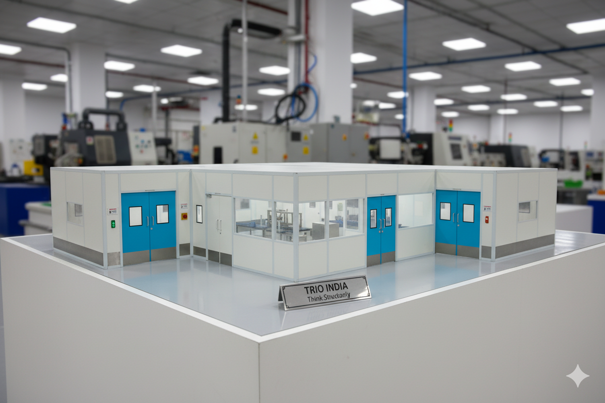
Cleanroom Panels & Partitions – Modular GI or aluminum panels with powder coating for easy cleaning.
-
Doors & Windows – Airtight cleanroom doors with interlock systems and flush vision panels.
-
HVAC & Pressure Cascade – Maintaining positive pressure to keep contaminants out.
-
Lighting & Flooring – LED lights with minimal heat emission and anti-static flooring.
5. Cleanroom Construction: Step-by-Step Process
Building a semiconductor cleanroom requires precision engineering.
-
Requirement Analysis – Understand ISO class, process needs, and contamination control requirements.
-
Design & Layout Planning – Optimize workflow, material flow, and personnel movement.
-
Fabrication of Modular Components – Panels, doors, windows, and ceilings.
-
Installation – Erect partitions, ceiling grids, and cleanroom accessories.
-
HVAC & Filtration Integration – Fit air handling units, ducts, and filters.
-
Electrical & Data Cabling – Install concealed cabling for safety.
-
Validation & Testing – Airflow, pressure, particle count, and certification.
At Trio India, our modular construction approach reduces project timelines by up to 30–40% compared to traditional builds.
6. Modular vs Conventional Cleanrooms in Semiconductors
-
Modular Cleanrooms:
-
Quick installation
-
Scalable and cost-effective
-
Flexible design modifications
-
-
Conventional Cleanrooms:
-
Better for large, permanent fabs
-
Time-consuming and costly
-
Limited flexibility
-
💡 Semiconductor companies increasingly prefer modular cleanrooms due to shorter time-to-market cycles.
7. Turnkey Semiconductor Cleanroom Solutions
Turnkey cleanroom solutions cover the end-to-end process: design, manufacturing, installation, and validation.
Advantages of Turnkey Solutions:
-
Single point of responsibility
-
Faster project delivery
-
Cost efficiency
-
Full compliance with ISO standards
👉 Explore Trio India Cleanrooms
8. Cleanroom Maintenance & Validation
A semiconductor cleanroom must be continuously monitored and validated.
-
Airflow Testing – Check laminar flow and velocity.
-
Particle Count – Validate against ISO Class standards.
-
Filter Maintenance – Replace HEPA/ULPA filters regularly.
-
Surface Cleaning – Use approved lint-free materials.
-
Temperature & Humidity Control – Maintain stability for sensitive processes.
-
Annual Re-Validation – Required for ISO compliance.
9. Common Challenges in Semiconductor Cleanrooms
-
Particle Contamination – From operators, tools, or air leaks.
-
Energy Efficiency – HVAC systems consume up to 50% of fab energy.
-
Scalability – Upgrading cleanrooms as processes evolve.
-
Compliance Costs – Meeting international ISO and GMP standards.
10. FAQs on Semiconductor Cleanrooms
Q1: What ISO class is required for semiconductor fabrication?
Most wafer fabs require ISO Class 1–5 cleanrooms depending on the process.
Q2: How much does a semiconductor cleanroom cost?
Costs vary widely depending on size, ISO class, and equipment – typically ₹50,000 to ₹1,50,000 per m² in India.
Q3: What’s the difference between semiconductor and pharmaceutical cleanrooms?
Semiconductor cleanrooms demand stricter particle control (nanometer level), while pharma focuses on microbial contamination.
Q4: Can modular cleanrooms be upgraded later?
Yes, modular cleanrooms are designed for scalability and process upgrades.
11. Conclusion: Building the Future of Chip Manufacturing
As semiconductors power the future of AI, EVs, and IoT, the need for world-class cleanroom facilities has never been greater. With the right semiconductor cleanroom design, construction, and maintenance strategy, manufacturers can achieve higher yields, faster time-to-market, and global competitiveness.
At Trio India, we specialize in turnkey modular cleanroom solutions for the semiconductor industry – from design to validation. Whether you are building a new fab or upgrading an existing one, our expertise ensures compliance, efficiency, and innovation.
👉 Contact Trio India today to explore customized cleanroom solutions for your semiconductor projects.